JVM Research & Technology
Electrical Engineering, emphasizing analog experience in design and development
JVM Research Home Page
JVM Research Electrical Engineering Home Page
JVM Research Display Engineering Home Page
PDP Driver Circuits
Designs are by Joe Miseli, 1998.
These are contributing work toward patent 6157375, "Method and Apparatus for Selective Enabling of Addressable Display Elements." This was a joint patent to provide a more efficient and reduced power method for driving PDP (Plasma Display Panels)pixel arrays. It could reduce the need for having individual drivers for every row and column.
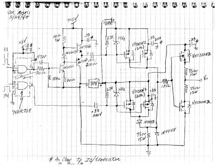
Above is the fundamental design. Note the 80V required per driver for the PDP technology. With that high voltage and the numbers of drivers required in conventional PDP driving, one can see the great power-saving advantage and circuit complexity reduction in having a concept that enabled reduction of numbers of drivers to a PDP display.
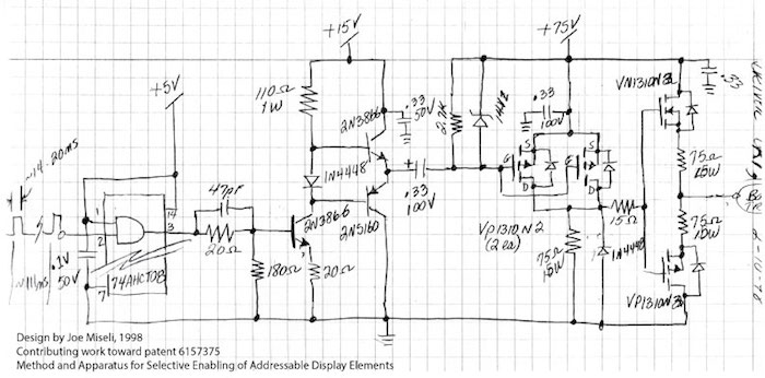
This is a variation.
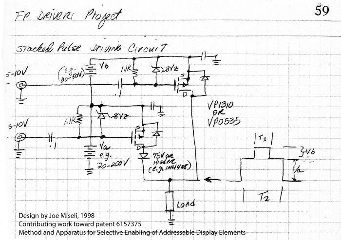
This is a stacked pulse driving circuit, a convenient way to produce a bi-level synchronizing pulse needed for the PDP driving.
Back to the JVM Research Electrical Engineering Home Page