JVM Research & Technology
Electrical Engineering, emphasizing analog experience in design and development
JVM Research Home Page
JVM Research Electrical Engineering Home Page
JVM Research Display Engineering Home Page
Delay Line Circuit
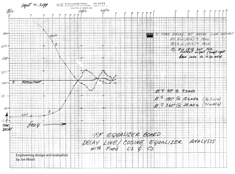
Design is by Joe Miseli.Delay lines are circuits which produce a designed amount of delay for a signal while assuring minimal gain or phase change, group delay, etc. They must be flat across the frequency of interest and have little or no roll off.
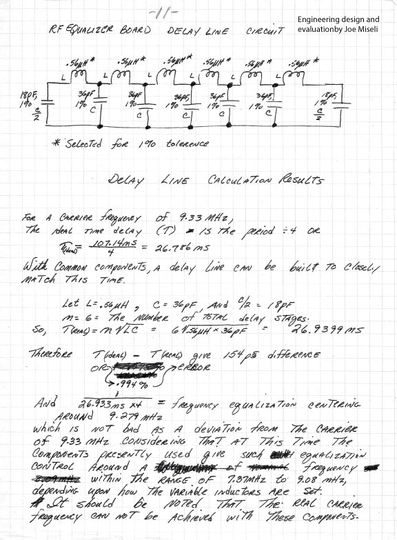
Above is the delay line design for a 9.33MHz delay line. Leaded components had to be measured and hand selected.
Below is a the validation of the design by measuring it and plotting it. Yes, in the old days, we had to measure performance (in this case time delay vs. frequency) point by point and manually plot it on semilog paper. Ug!